顯示具有 arm 標籤的文章。 顯示所有文章

2024年6月15日 星期六

在 ARM 平台上使用 Function Multi-Versioning (FMV) - 以使用 Android NDK 為例

Function Multi-Versioning (FMV)

過往的 CPU 發展歷程中, x86 平台由於因應各種應用需求的提出, 而陸陸續續加入了不同的指令集, 此外也可能因為針對市場做等級區隔, 支援的數量與種類也不等. 在 Linux 平台上這些 CPU 資訊可以透過 /proc/cpuinfo 取得. 而對於 CPU 不同的指令集支援去實作軟體最佳化, 是相當繁複的工作. 而這些在過去分享過的 Function Multi-Versioning (FMV) 的出現, 而大幅地簡化.

隨著時間過去, 這十年來發展迅速的 ARM 平台, 在 ARMv8 之後不斷作小幅度的翻新, 也逐漸產生類似 x86 平台上的問題. 以 A-Profile 處理架構而言從 ARMv8.0-A 一路發展到 ARMv9.4-A. 當中有著許多新硬體特性與新增指令, 有些是 core feature 而有些則是 optional, 這些也逐漸造成了 ARM CPU 平台功能性上大小不等的碎片化. 在 ARM 官網有提供了一份 "Feature names in A-profile architecture" 列表. 而這整理僅止於 ARMv9 之前. 此外更麻煩的地方是, 各大 compiler 在先前一直沒有對應支援 FMV 的功能, 如此對於通用的應用程式, 想要能夠有效使用 ARM 這些功能特性同時顧及不支援的平台, 著實是一件不簡單的事.

而事情在 2023 年中開始有了轉機, 在當時所釋出的 Clang / LLVM 16.0 開始在 ARM 平台上支援  FMV 功能. ARM 官方甚至在其系列文的 "What's new in LLVM 16" 中有特別舉例說明 FMV 的使用. 一旦能夠使用 FMV, 這對於不確定運作的目標平台的應用程式開發很有幫助. 但在當時個人第一時間找不到具有支援的 llvm toolchain, 而之後的這段時間因工作繁忙一直沒有時間再繼續做嘗試, 也就沒辦法撰寫心得. 近日回想起心中所惦記的這麼一件事, 於是特別拿了最新的 Android NDK 26d (附的是 clang 17.0.2) 來測試.

Case Study - FP16 GEMM w/ Vector Extension, Gather Auto-Vectorization

首先請安裝 Android NDK 26d 到 /opt 目錄內, 並將 /opt/android-ndk-r26d/toolchains/llvm/prebuilt/linux-x86_64/bin/ 加入 PATH 環境變數中.

由於個人在過去所分享的教材投影片中即談論過 FMV, 本文中就不再多做詳細介紹, 有需要可以參考過去的投影片, 在這裡就透過兩個實際的例子來嘗試 ARM FMV 功能, 第一個 Case 是個人常拿來作為 Compiler Vector Extension 的 Laboratory 範例的 Matrix Multiplication, 這個範例可以顯示出使用 Compiler Vector Extension 搭配 FMV 可以共伴產生廣泛支援又高效的程式碼:

typedef __fp16 fp16_16 __attribute__((ext_vector_type(16)));
#ifdef __HAVE_FUNCTION_MULTI_VERSIONING
__attribute__((target_clones("sve2", "simd")))
#endif
void gemm_vec(
    // buffer, stride
    __bf16 *a, int sa,
    __bf16 *b, int sb,
    __bf16 *c, int sc
){
    fp16_16 vb[16];
    for(int y = 0; y < 16; y++){
        vb[y] = *((fp16_16*)(b + sb*y));
    }
    for(int y = 0; y < 16; y++){
        fp16_16 vc = *((fp16_16*)(c + sc*y));
        fp16_16 va = *((fp16_16*)(a + sa*y));
        for(int x = 0; x < 16; x++)
            vc += va[x]*vb[x];
        *((fp16_16*)(c + sc*y)) = vc;
    }
}

這個範例中, 為了能產生較大的 code generation 的差異, 個人選擇使用 float16 的資料型別. 主要是因為 ARMv8 並非預設支援 fp16, 而是到了 ARMv8.2 以 optional extension 來提供 (而預設支援 SVE2 的 ARMv9 是預設支援的). 將上述這段程式令存為 arm_gemm.c 之後搭配下列指令編譯:

$ aarch64-linux-android34-clang -O3 --save-temps -c arm_gemm.c
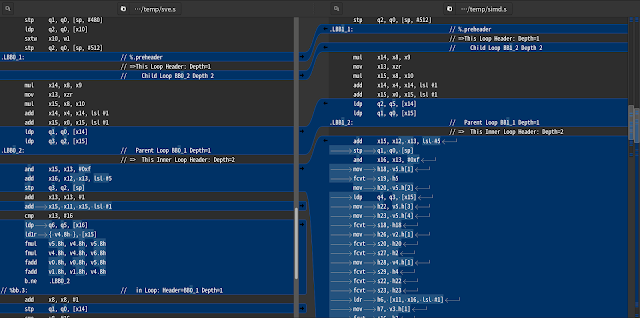
如此當中可以觀察產生的 arm_gemm.s 檔案, 當中有 gemm_vec._Msve2 與 gemm_vec._Msimd 兩段程式, 以及用來做選擇的 gemm_vec.resolver, 可以觀察 sve 版本直接使用支援 fp16 的 fmul, 而 AdvSIMD 版本當中不斷使用 fcvt 指令來處理浮點數轉換, 行數落差也相當的大.


接著的第二個範例中是透過 auto-vectorization 來實際展示 ARM 官網上的 "Auto-vectorization examples" 內關於 Scatter and Gather 的部份, 而為了能確實透過 clang/llvm 的組合產生使用 gather 指令, 該段程式經過稍加修改後程式碼如下:

#include <stdint.h>
#ifdef __HAVE_FUNCTION_MULTI_VERSIONING
__attribute__((target_clones("sve2", "simd")))
#endif
float gather_reduce(float *restrict data, int *restrict indices, long c)
{
    float r = 0;
    #pragma clang loop vectorize(enable)
    for (long i = 0; i < c; i++) {
        r += data[indices[i]];
    }
    return r;
}

將上述這段程式令存為 arm_gather.c 之後搭配下列指令編譯:

$ aarch64-linux-android34-clang -O3 --save-temps -c arm_gather.c
同樣地, 透過觀察編譯過程中產生的 arm_gather.s 檔案, 當中有 gather_reduce._Msve2 與 gather_reduce._Msimd 的兩段程式碼, 從中可以看到 SVE 的版本的 gather_reduce function 確實有使用 L1DW 這個 SVE 指令集所專屬的 gather 指令.

ARM Feature List

最後談談 ARM 與 x86 平台在 FMV 在實務使用中不同的地方. 在 ARM 平台的 FMV target 僅止為 feature, 而 x86 FMV 的 target 則能夠是特定的 CPU arch, 特定的 CPU core 或是指定的 ISA. 那麼具體來說在 ARM 上 FMV 有哪些 feature 可以選擇呢? 可以參考ARM 這份 ACLE 文件, 當中有提供對應的 feature 列表與在指定 FMV target 的名稱, 另外如以往的 FMV target 的使用, 這些 feature 是可以透過 + 來合併選擇使用的, 像是 "sve2+memtag" 來合併使用 SVE2 與 Memory Tagging, 同樣地一如以往 "default" 表示的是基本的指令集, 產生完全不會使用到 feature 的 code.

2022年3月12日 星期六

ARM SVE 研讀筆記 Part-6 - Extended floating-point horizontal reductions 與 SVE/SVE2 optionals

這篇是系列文的最後一篇, 主要談兩個列於標題的項目.

Extended floating-point horizontal reductions

在討論 Extended floating-point horizontal reduction 時必須要知道 ARM 在 ARMv8 時增加了一些 instruction / intrinsic functions. 從官方的 ARM NEON intrinsics reference 可以查找出這次要討論的主角 vaddvq_f32 / vaddvq_f64. 這兩個 intrinsics 的目的在於把向量中所有 float / double elements 加總回傳. 雖然相當簡單, 但是 floating-point 的操作對於驗證有個很重要的議題 - order. 透過 reference 查找出此兩者, 可以得知在 ARMv8 是透過 FADDP 指令來達成的. 這個指令是將相鄰的成對數值相加. 從 vaddvq_f32 可以看出是利用兩個 FADDP 指令達成加總的目的. 這樣做的好處是可以減少 instruction latency. 然而這樣的次序在驗證上需要特別處理.

Fig. 1 - SVE 同時提供了 floating-point  in-order 與 tree-based reduction 處理

在 SVE 中同時提供了 in-order (由左至右) 與 tree-base (成對相加) 的作法. 如此可以取決於效能還是結果驗證從這兩者選擇. 在 ARM C Language Extension 可以看到下列的段落:

Fig. 2 - 兩種不同順序浮點數加總的 SVE intrinsic function

依照先前說明轉換 NEON intrinsics 至 SVE intrinsics 的規則, 可以輕易的了解 NEON 中的 vaddvq_f32 對應的 SVE intrinsic function 為 svaddv_f32. 也映證了原有的方式是基於效能的 tree-based. 而新增加的是由左至右的作法是 svadda_* 系列. 而由於 in-order 的特性, 在執行上也較為沒有效率, 從 Arm Cortex-X2 Core Software Optimization Guide 可以看出 FADDP 與 FADDA 兩者有著相當大落差的 exec latency (也就是需要幾個 CPU cycle 才能產生所需結果)

SVE/SVE2 options

在 ARM 制定 SVE 的過程中, SVE 與 SVE2 各自有其核心目標, 這篇主要是說明 SVE 到 SVE2 制定上功能上的演進. 搭配 ARM A-Profile 網站與 ARM C Language Extension 文件閱讀會比較有感.

Fig. 3 - SVE Base functions

SVE base 中建立了 SVE Programming Model 的基本需求. 基本上大部分的 intrinsic functions 都會落在這個類別.

Fig. 4 - SVE optional

在 ARMv8.6 提出時對於 SVE 增加對 BFloat 16 與 GEMM 的支援. GEMM 上主要是能以 vector 來完成 8x2 & 2x8 (8bit) 或是 2x2 (floating-point) 的 Matrix Multiply. 詳情建議閱讀官方 Blog 介紹文章. 值得一提的是 SVE option 的提出時間點 (ARMv9.1) 比 SVE2 推出的時間(ARMv9.0)還晚.

Fig. 5 - SVE2 Base 新增功能列表

將 SVE 列為核心功能是在 ARMv9.0 的事情, 當時是以 SVE2 的版本加入. 相較於一開始與 Fuji 合作於 A64FX 超級電腦核心的 ARMv8.2 中採用的 SVE 已有相當的時日. SVE2 很大的部份在補足 SVE 設計上的缺漏. 特別是在 SVE 中缺少的 data width widening & narrowing 的運算. 另外像是 while loop control 對於 decremental counter 的支援, 複數與大數的支援等等 ...

Fig. 7 - SVE2 optional 增加的功能

最後是 SVE optional functions, 這一部份主要集中於 Crypto 應用的部份. 透過這些指令可以加速 AES-128, SHA-3  與 SM4 的加解密應用. 另外是一個較大的 extension - SME. SME 基於 SVE / SVE2 提供了更有效處理 Matrix 操作的功能. 除了提供 outer-product engine 外也額外增加新的執行模式 - "Streaming Mode". 軟體實作可以藉由使用這個模式來支援更大的 vector length 與達到更高的 throughput. 詳情可以參考 ARM 官方 SME 介紹文.

至此大略介紹了 ARM SVE/SVE2 的功能與相關 extensions. 後續希望有機會在撰寫相關實務文章.

2022年3月4日 星期五

ARM SVE 研讀筆記 Part-5 - Gather & Scatter

在 Processor 中開始出現 Gather and Scatter 相關指令之前之前, 許多 Hardware IP 就俱備有 Gather & Scatter DMA. 像是由於影像處理的需求, 一些 DSP 就俱備 2D DMA, 許多商業市場上的應用 DSP 都俱備這種能力(e.g: CEVA, Cadence Tensilica, Synopsys Arch ...), 而因為近年的 ML 對於 Tensor 操作的部份, 所以像是 >= 3D 或是俱備更多操作彈性的 DMA 在這幾年之中都出現了. 而 ARM SVE 迎合這個發展方向與相關的應用, 在推出時也針對 vector loading 做了補強, 增加了 Gather & Scatter 的相關指令.

Fig. 1 - Gather & Scatter 示意圖

首先必須說明 Gather 與 Scatter 的意義為何, 這是兩個對應的動作. 所謂的 Gather 是透過硬體所提供的規則將指定不連續的資料於 load in 後整併為單一個 vector 的動作; 而 Scatter 則是一個反向的行為, 也就是將所指定的 vector 中的資料, 透過規則所指定的方式, 將資料存放到各個不連續的記憶體位置中. 以這樣的方式看來 ARM NEON 原本就俱備的 vld2/vst2, vld3/vst3 與 vld4/vst4 事實上也是一個規則固定的 Gather / Scatter 退化型操作.  然而 vldN / vstN 因為規則太過固定, 因此實用性還是有所侷限. (話說 vld3 其實相較 x86 的 SSE/AVX 對於 3-channel 的資料, 像是 RGB/YUV 等等的操作真的方便不少)

Fig. 2 - LD1 scalar base, vector offset 的例子

在 ARM 官方的文件 ARM C Ext. for SVE 中, 對於 Gather / Scatter 並非是匯整在同一個章節, 相對地這些是分散在 6.2 Loads 與 6.3 Stores 兩節中. 對於 Gather / Scatter 中提供不連續記憶體位置的方式有三:

  1. base only: 也就是每個 lane 使用對應 lane 指定的 address
  2. base + offset: 每個 lane 的 address 計算方式為: base + offset (in bytes) 的方式
  3. base + index: 每個 lane 的 address 計算方式為: base + index (of element) 的方式, 也就是位置計算是 index * sizeof(element)

Fig. 3 - AoS 與 SoA 的不同考量示意

而 2. 與 3. 當中的 base  + offset/index 的組合有著 (scalar, vector) 或是 (vector, scalar) 的組合, 一共有 4 種類型. 從使用面向上來看這兩種有著不同的應用:

  • scalar base + vector offset/index - 使用單一的 base, 搭配個別的 offset/index, 也就是說這適合單一起點的 structure of arrays 的方式
  • vector base + scalar offset/index - 使用單一的 offset/index, 搭配個別的 base, 也就是說這實際上非常適合應用在讀取 array of structures.


Fig. 4 - Vector Address 計算的相關 intrinsic 說明

最後是輔助 Gather & Scatter 的 vector address 計算的功能, 在 ARM SVE 中提供了 ADR 以及 INDEX 這兩個指令, 前者提供了 per-lane 的個別計算, 後者是以 base 與 steps 兩個參數來規律地計算產生整個 vector (事實上這個 index function 也可以用在需要等差級數的 vector 時候, 像是 shuffle 這類的情況)

下一篇會進入 ARM SVE 研讀筆記的最後一篇 Part-6, 除了介紹最後一個功能特性 - extended floating-point horizontal reductions 之外也討論 SVE / SVE2 各自涵蓋的功能特性範圍.


2022年2月28日 星期一

ARM SVE 研讀筆記 Part-4 - Predicate-driven loop control and management 與 Vector partitioning & software-managed speculation

Predication-driven loop control and management

Fig. 1 - Part-3 中使用的 ARM 官方 SVE 範例

事實上在 Part-3 的 ARM 官方範例中, 就已經展示了這個特性, 在 ARM SVE 中提供了 WHILELT 與 WHILELE 指令來作為遞增 for loop 中的 > 與 >= 的比較, 並產生對應所需的 predication 結果來處理在一般 SIMD 當中較不方便處理的 loop 結尾, 這是由於 loop 的結尾所需處理的數量很可能並非是 vector-size 的倍數, 而記憶體存取的位置也很可能並非 vector-size aligned. 在範例中可以看到使用了 svwhilelt_b64, 這即為 SVE 提供的 loop control / management 功能. 在 ARM SVE  中針對處理資料寬度提供了各自對應的 intrinsic functions:

  • 8bit - svwhilelt_b8 / svwhilele_b8 / svcntb 
  • 16b -  svwhilelt_b16 / svwhilele_b16 / svcnth
  • 32b - svwhilelt_b32 / svwhilele_b32 / svcntw
  • 64b - svwhilelt_b64 / svwhilele_b64 / svcntd

而在 ARM SVE2 中針對遞減 for loop 增加了 WHILEGT 與 WHILEGE, 很直覺地這是用來處理 loop control 中的 < 與 <= 的比較.

  • 8bit - svwhilegt_b8 / svwhilege_b8 
  • 16b -  svwhilegt_b16 / svwhilege_b16
  • 32b - svwhilegt_b32 / svwhilege_b32
  • 64b - svwhilegt_b64 / svwhilege_b64

Vector partitioning & software-managed speculation

在許多時候 buffer 的長度並非 vector size 的倍數, 這造成 vector load 的行為可能會超過 buffer 邊界, 或是要處理的資料的長度未知, 可能在處理過程中造成 memory fault 的行為. 而在讀取過程中, 可能有因計算需求的其他對應的 vector load. 對於這樣的需求, ARM SVE 導入了 First-Faulting 與 Non-Faulting vector load 的設計.

Fig. 2 - ARM SVE 使用的 register set

在 ARM SVE 的 register set 中有著一個不起眼的 register - first-fault register (FFR), 其寬度與 predicate register 相同. FFR 的目的在於存放執行 first-faulting or non-faulting vector load 中每個 lane 成功與否的結果. 

Fig. 3 - first-fault register 運作機制

而 first-faulting 與 non-faulting 的差異在於 first-faulting vector load 的 VLDFF1 系列指令中, 只有第一個 active lane 會產生造成例外情形的 memory fault. 而 non-faulting vector load 的 VLDNF1 系列指令按照字義上而言就是不會產生 memory fault 的指令. 此外, 無論使用 first-faulting 或是 non-faulting vector load 的時候, 在 FFR 中每個 lane 對應的值若事先已被設為 0 / false, 那麼該 lane 的結果將會是 unknown 狀態. 

Fig. 4 - First-Faulting Vector Load 範例

在 Fig. 4 中為 ARM C Language Extension 對於 first-faulting 的範例. 一開始執行 SETFFR 之後, FFR 的所有值都會為 1/true, 接著連續執行三次 LDFF1 指令, 將指定資料讀取至 Z0 ~ Z3. 最後透過 RDFFR 指令將 FFR 的內容存放至 P3 當中. 而 P3 所存放的數值表示哪些 lanes 在 Z0 ~ Z3 當中皆為 valid 狀態. 此資訊對於一些不定數目但需要合併處理的情況相當有幫助.


3/21 - 感謝來自 FB 臉友 王北北 的指正, SVE 與 SVE2 支援的 WHILELT&WHILELE 與 WHILEGT&WHILEGE 一時不察寫反了, 已修正

2022年2月26日 星期六

ARM SVE 研讀筆記 Part-3 - Per-lane predication

在切入 ARM SVE 第二個特性 - Per-lane predication 之前, 讓我們先以 ARM 官方 SVE 範例程式為例, 說明 SVE 的  C/C++ 程式看起來會是怎樣的型態.

使用 SIMD Intrinsics 依然是性價比相當高的方式, 除了可以直接與 C/C++ 程式碼混合撰寫外, 也避免了直接使用 assembly 撰寫的曠日費時與難以除錯. 當然使用 SIMD intrinsics 的缺點是可攜性與跨平台問題. 這點就在先前文章多少提及, 在此就不綴述. 這裡讓我們以第一個範例來切入 SVE intrinsics 的使用

Fig. 1 - SVE  intrinsics 使用範例程式 double dot

Fig. 1 中的程式來自 ARM 官方 SVE intrinsics 的範例, 這當中有幾個重點:

  • 首先是第一行藍色標示的部份, "arm_sve.h" 的使用對 SVE intrinsics 是必要的
  • 在上一篇有談到 SVE vector type 型別的使用來宣告變數, 上圖中以草綠色標示
  • 如同一般的 ARM NEON 程式, 呼叫所需要的 intrinsic function, 這裡以暗紅色標示. 值得一提的是, 雖然相較於 NEON intrinsics,  SVE 增加了 postfix 來做特定用途. 但多數基本功能, 都可以將 ARM NEON intrinsics 原有的名稱在開頭加上一個 "s" 並且移除用來判別處理 64/128-bit 寬度的 "q", 就可以索引到所需的功能. 例如, 原本做 float 型別的vector element 總和會使用 vaddvq_f32, 這裡就可以去搜尋到 Fig. 2 中所列出的 svaddv_f32
  • 最後是紫色標示的部份, 這也是本文要說明的 Per-lane predication, 在 ARM SVE 中新增了在 DSP SIMD 中常見的 Per-lane predication, 這能用來做更為細緻的控制, 來減少在程式撰寫中因 SIMD 限制而不得不以 scalar code 來處理的部份. 這個範例精簡地展示了 predicate 用在 SVE 中的 3 個 predication 特性 - 本文的 per-lane predication 與後續的Predicate-driven loop control and management 與 Vector partitioning & software-managed speculation.
Fig. 2 - 透過 NEON vaddvq_f32 能找到的 SVE intrinsics 系列

所謂的 Per-lane predication 功能是指在 SIMD 中在套用的操作上, 對於每個 lane 提供一個 bit 來做 active or inactive 的控制. 而 active lane 即表示需要直接套用所使用的操作. 對於 inactive lane 部份則有幾個模式, 這點會在稍候解釋.

Fig. 3 - predication 圖示

在 ARM SVE 的設計上對於多數 intrinsic function 都加入了 svbool_t 型別的參數 pg, 這即是用來作為 lane control 的 predication. 其基本概念如 Fig. 3 所示, 一旦該 lane predication 值為 1/true 的即表示該 lane 狀態是 active; 而若該 lane 的 predication 值為 0/false 的, 該 lane 狀態即為 inactive. 若 intrinsic function 沒有特別的 postfix, 那麼 inactive lane 則是維持原本的數值.

Fig. 4 - Predication register 對應 Vector register 的方式.

若對 Part-1 的內容還有印象的話, ARM SVE 的 vector register 為 128b 的倍數, 可為 128~2048b 的任何選擇. 而 predication register 為 16b 的倍數, 可為 16~256b 的任何選擇. 但 predication register 與 vector register 長度的關係是連動的. 一旦決定了 ARM SVE 中關於 vector length 的 LEN 參數, 就固定了兩者的長度. 這也表示 vector / predication 是以 8:1 的比例對應的. 對於 8b 以上的型別會有額外的 bit. 這時的選擇方式如 Fig. 4 所圖解的, 對於 16/32/64b 的 data types, 是以對應的多個 bits 之中最低位的 bit 來控制該 lane.
Fig. 5 - Predication 產生與操作的方式

到此可以輕易地理解, Predication 通常是用來處理 SIMD 中通常難以處理的 if/else 或是 switch case 等等的流程. 因此 predication 的產生最直觀的就是對應 C++ boolean type 中的許多 logical operations - 舉凡數值間各種比較運算 !=, ==, <, <= , >, >= 與 boolean type 間各類 !, &&, || 等等.

Fig. 6 - Inactive Lane 的模式

最後是 inactive lane 的動作, 依照所使用的 intrinsic function 共有 3 種, 也就是在一些 intrinsic functions 的名稱中在 data type 之後還可以看到 "_z", "_m" 或是 "_z" 的 postfix. 這是對於 inactive lane 模式的選擇. 使用了 "_z" 結尾的 intrinsic function 表示了希望 inactive lane 的數值填為 0; 而使用了 "_m" 結尾的 function 則是代表維持原本輸入的第一個 vector 參數並不做任何的更動; 最後是 "_x", 這表示不在意 inactive lane 的數值, 讓 compiler 去針對 compilation 參數(performance or code size)去作較佳的選擇( _z, _m 或是甚至不使用 predication ), 一旦使用 "_x" 的 intrinsic function 必須清楚地知道, inactive lane 當中並沒有預設或保證當中為何值.

下一篇將延續 Per-lane predication 來同時講述 Predicate-driven loop control and management 與 Vector partitioning & software-managed speculation.


ARM SVE 研讀筆記 Part-2 - Vector Length Agnostic (VLA)

個人認為 Vector Length Agnostic (VLA)  是討論 SVE 時必須先討論的特性. 談到這特性必須先了解多數的 SIMD 指令集都有固定使用的 vector width/length, 像是 intel 對於 x86 平台的 SIMD 發展過程, 從 MMX 的 64-bit 開始, 一路發展 SSE / 128-bit , AVX & AVX2 / 256-bit 到最近的 AVX-512 / 512-bit 每一組都有固定的 vector length, 但是即便使用相同的運算, 對於使用了不同的 SIMD instruction set, 這也必須對應到 CPU 內不同的 opcode. 因此使用舊的 SIMD instruction 的程式並無法受益於新一代 SIMD ISA 的好處.

而 ARM SVE 在制定時一開始就允許 IC 商能夠依照應用的需求的考量, 去配置硬體內的 SIMD vector length. 另外制定 SVE 專屬的 VLA vector type 與 intrinsics, 讓開發者能夠達到撰寫所撰寫的 ARM SVE 程式無需特別針對 vector length 改寫或重新編譯, 即可執行運作. 而 IC vendor 也能更為安心地藉由增加 vector length 達到效能增加而無需擔心程式的重新客製問題.

Fig. 1 - Vector Length Agnostic 的圖解與程式特性

類似於其他各 SIMD 指令集的 C intrinsics, 需要對應的 vector type 與 intrinsics function. ARM 對於 SVE,  也提供了對應的 vector type 以及 function 介面. 如 Fig. 2 中所列出的, 其 vector type 涵蓋了基本的 8/16/32/64-bit signed / unsigned int 與 float / double 等等, 然而還增加了 boolean, float16 與 bfloat16 等等新的型別.
Fig. 2 - ARM SVE intrinsics提供的 vector types

然而這些 Vector types 與其他 SIMD intrinsics 所提供的最大不同是這些是 "sizeless", 也就是對於 compiler 而言,  這些 vector types 並沒有俱備任何 size 資訊. 於第一時間或許覺得沒大問題, 但是事實上 VLA 帶來了許多在語言特性以及工具使用上的限制: 

Fig. 3 - Sizeless 帶來的實務限制

如 Fig. 3 所列出的, VLA 帶來的限制主要都是因為缺乏 size 資訊造成需要此資訊的語言特性使用的限制. 這些包含了無法去使用 sizeof / alignment, pointer arithmetic. 比較不直覺的像是無法作為 union / struct / class 的 member field 與宣告用來存放的 STL container , 另外無法成為 exception handling 中 throw / catch 機制的 object. 最後是 lambda 中 capature 機制無法 capture by value. (但是能夠使用 capture by reference )


2022年2月16日 星期三

ARM SVE 研讀筆記 Part-1 - ARM SVE 基本概述

ARM 於 ARMv8.2 時期開發了新一代 SIMD 指令集, 以選擇性擴充的方式來接替已使用多年的 NEON, 並在 ARMv9 中預設涵蓋, 該 SIMD ISA 全名為 Scalable Vector Extension 簡寫為 SVE. 這中中最著名的使用案例是與富士合作的 ARM 超級電腦平台中使用了配置為 512b vector length 的 SVE 實作. 相較 NEON 而言, SVE 除了新增功能特性的設計上, 除了增進便利性, 也同時一併考慮了 SIMD 效能擴充 / 延伸性的問題. 

Fig.1 - ARM SVE vector register 與 NEON register 關係圖.

ARM SVE 的設計最特別的地方在於它採用了不同於現今主流 CPU / DSP 皆以 fixed vector length 來制定出一組 SIMD 指令集的方式. 在設計上採用了硬體實作中可對於內部 vector length 作可調整配置的方式, 這也是名稱上使用了 "Scalable" 一詞的原因. ARM SVE 允許硬體商因應用效能上需求的考量而去決定 vector length, 越長的 vector 因為需要更多的 ALU 來提供 ILP, 也會直接地反映在 die area 上. 而 ARM SVE 的 vector length 選擇上必須是介於 128~2048b 而且為 128b 的倍數.

Fig. 2 - ARM SVE 新增的 predicate register.
設計上與 ARM NEON 的另一個重大差異, 在於 ARM SVE 導入 16 個 predicate register.  這是用在於 DSP SIMD 中相當常見的 Per-lane predication 用途上. 在此必須特別說明的是於 Fig. 2 中的 LEN 參數與 Fig. 1 的是連動的相同數值, 這表示 IC vendor 選擇了 LEN 就同時固定了 vector 與 predicate register 的長度, 因此兩者長度的比例固定為 8:1. 在 ARM SVE 中透過使用  predicate, 能夠精確的控制個別資料的計算與否, 如此處理一些 if/else 等等的狀況會更為便利. 由於 SVE 的進階功能都圍繞著 predication 的使用, 因而 SVE 也有著對 predication 運算操作的指令.
Fig. 3 - 總結 ARM SVE 的重大特性

個人統整認為 SVE 的主要特性有 1(個人認為應該加入) + 5, 分別是:

  • Vector Length Agnostic (VLA)
  • Gather-load and Scatter-Store
  • Per-lane predication
  • Predicate-driven loop control and managment
  • Vector partitioning for software-managed speculation
  • Extended floating-point and bitwise horizontal reductions.

後續陸續將這些心得一一分享. 下一篇將介紹說明 Vector Length Agnostic (VLA)

2021年2月28日 星期日

Raspberry Pi Zero W Project Part 3 - Software Interrupt & Handler example

For ARM architecture, the instruction for software interrupt is SWI or SVC (ARMv7).

Using the instruction is very simple:

SVC #imm

When an ARM processor executes the instruction, it will switch to SVC/SWI mode and jump to the SWI or SVC hander in exception vector table specified by Vector Base Address Register (VBAR).

Similar to previous parts, please get from repo https://github.com/champyen/rpiz_bare_metal.git 

please checkout the commit: 637086c2

$ git checkout 637086c2

It is not difficult to use SWI/SVC instruction. But it requires experience to apply it well. Using SWI/SVC instrution for system calls, we need to:

  • design system call table ( SWI number , system call pair)
  • implement SWI/SVC handler, get the system call number
  • implement system calls with corresponding number

For get the SWI (or system call) number, it is describe in ARM's "SWI Handler's" document. The SWI number is encoded as lowest 24 bit in SWI/SVC instruction. Therefore we could get SWI/SVC number by fetching the instruction itself and clearing the MSb 8bits with BIC instruction right after entering SWI hander:

ldr     r0, [lr,#-4]
bic     r0, r0, #0xff000000

After getting SWI number, we could pass it to system_handler as an argument saved in R0. The system_hander is very similar to ISR, but we don't need to check the hardware status to know which hardware interrupts CPU. We just need to handler the SWI or system call by the SWI number. Of course, as IRQ has Interrupt latency SWI/SVC instruction consumes more cycles than normal instructions for most CPUs.

For Application processor it is easy to understand the meaning of mode switching and SWI handling. In fact, Cortex-R, and Cortex-M processor also has SWI/SVC instruction. For most Embedded / RTOS developers, they think it is useless or trivial in such processor.

For some embedded or RTOS, mutual-exclusive applications can be loaded on demand. This can be done by well-designed linker-script (e.g.: different LAs with same). For such Embedded / RTOS, SWI / SVC instruction is useful to maintain an API layer between Applications and Kernel. An intuitive / naive way is to setup and maintain table of function pointers on the kernel side (Of course we still need to setup API index for using the function as SWI number). For development it has an drawback: it is hard to maintain or adjust or expand the table. With SWI/SVC instruction, no table forwarding is needed. Besides it provides flexibility to group system calls and reserve numbers for future needs. (Since for table-based method, it required to reserve a huge table).


2021年2月6日 星期六

Raspberry Pi Zero W Project Part 2 - Interrupt Service Routine (ISR) example

After implementing naive function and printf, let's add ISR to it.

please checkout the commit: 91abc0d3

$ git checkout 91abc0d3

There are many changes from previous commit:

head.S

it becomes more complicated. As we know, its context starts at 0x8000 address.

start:
    ldr     pc, reset_target        /* 0x00 mode: svc */
    ldr     pc, undefined_target    /* 0x04 mode: ? */
    ldr     pc, swi_target          /* 0x08 mode: svc */
    ldr     pc, prefetch_target     /* 0x0c mode: abort */
    ldr     pc, abort_target        /* 0x10 mode: abort */
    ldr     pc, unused_target       /* 0x14 unused */
    ldr     pc, irq_target          /* 0x18 mode: irq */
    ldr     pc, fiq_target          /* 0x1c mode: fiq */

reset_target:           .word   reset_entry

undefined_target:       .word   undefined_entry
swi_target:             .word   syscall_entry
prefetch_target:        .word   prefetch_entry
abort_target:           .word   abort_entry
unused_target:          .word   unused_entry
irq_target:             .word   irq_entry
fiq_target:             .word   fiq_entry

After loading the binary, it will jump to a routine named "reset_entry". Before we trace the reset_entry. The 8 "ldr pc, XXXXXX" instructions are so called Exception Vector Table. (FIQ is a special irq mode, it has a advantage - the implementation can be start at the location, the jump is not necessary. Therefore one jump delay is saved. ) It is used to handle system exceptions. Each has corresponding privileged mode to it. Besides, each mode has dedicated LR and SP registers - this means OS / firmware implementation should take care of stack space arrangement for the mode:


In fact, for reset_entry here, its major work is setting stack for each mode:

reset_entry:
    /* set VBAR to 0x8000 */
    mov r0, #0x8000
    mcr p15, 0, r0, c12, c0, 0


    /* (PSR_FIQ_MODE|PSR_FIQ_DIS|PSR_IRQ_DIS) */
    mov r0,#0xD1
    msr cpsr_c,r0
    ldr sp, stack_fiq_top

... other 4 modes ...

    /* (PSR_SVC_MODE|PSR_FIQ_DIS|PSR_IRQ_DIS) */
    mov r0,#0xD3
    msr cpsr_c,r0
    ldr sp, stack_svc_top

    cpsie i
    bl  bare_metal_start

In addition to stack assignment and jump to bare_metal_start , there are two key points here:

  1. setup Vector Base Address Register (VBAR) - From ARMv6, the exception vector can be placed other than 0x00000000 and 0xFF000000. This is achieved by setting VBAR, please refer to "3.2.43 c12, Secure or Non-secure Vector Base Address Register" in ARM1176JZF-S TRM.
  2. enable interrupt - cpsie instruction

And we have to trace isr_entry:

irq_entry:
    stmfd  sp!, {r0-r12, lr}
    add     lr, pc, #4
    bl      isr_entry
    ldmfd   sp!, {r0-r12, lr}

    subs    pc, lr, #4
For ISR, it is not surprised to backup and restore all (non-dedicated) registers. The most interesting things are - LR register setting and the instruction to leave IRQ mode. For LR setting it is easy to figure out, the target return address is the 'bl isr_entry' not 'add lr, pc, #4". That's the main reason to save "pc+4" to LR. And for leaving each mode, please refer to "2.12.2 Exception entry and exit summary" of ARM1176JZF-S TRM.

isr.c

There 3 functions in the source file: timer_enable, timer_check and isr_enty. Here we use "System Timer" in BCM2835, please refer to Chap 7 and Chap 12 of "BCM2835 Peripheral specification". Besides the IRQ number of System Timer is not listed in the document, please refer to the link of  "errata and some additional information" on the page.

The timer_enable will enable System Timer 1 or 3 by index and timer_check is used to clear IRQ state and update next timeout interrupt. Therefore the isr_enty just check status and call timer_check for clear the IRQ.

bare_metal.c

For demonstrate IRQ and main thread's progress, a busy loop with counter is added. The loop will print out a number when specified condition is met. And Timer is enabled before the loop, You can see the timer tick with ISR and the main thread keeps counting.

void bare_metal_start(void)
{
    int base = 0;
    asm volatile (
        "mov %0, sp\n\t" : "=r" (base)
    );

    printf("\n\n%s:%x: Hello World! %s %s %d\n\n", __func__, base, __DATE__, __TIME__, __LINE__);
    printf("enter busy loop\n");

    timer_enable(1);

    volatile int i = 0;
    while(1){
        if((i++ & 0x00FFFFFF) == 0)
            printf("%d\n", i);
    }

}


2020年12月29日 星期二

Raspberry Pi Zero W Project Part 0.5 - Documents

Documents

Before starting the project, to collect documents is an important things. 

It is important to study document before and during implementation.

The documents needed in the project are:

1. Raspberry Pi's Official Documents

2. Broadcom BCM2835 Peripheral specification

3. ARM1176

BCM2825 Address Space


It is important to know the address view of CPU and VPU/GPU. You have to know the difference between physical address and bus address of BCM2835. Otherwise you can't get hardware work correctly.

Why Raspberry Pi Zero WH?

The reasons of selecting RPi ZW as my project platform are:

  1. cheap, easy to get one, ARMv6 provides enough features of modern ARM Application processors.
  2. single core, simple & good for teaching / practice.
  3. low power, RPi ZW can be powered by almost any USB slot.
  4. RPi has a lot of documents / projects / implementations for reference.

What's in Next?

In next part, simple assembly programming on RPi Zero W will be introduced. We need to use assembly to implement some important parts of OS and bootloader.

2018年7月11日 星期三

開源陣營對 ARM 的回應 - www.arm-basics.com

延續上一篇文章 ARM 對 RISC-V 發起的攻擊
朋友稍早傳來一個網址 - https://www.arm-basics.com/
裏面有著針對 ARM 提出的攻擊的回覆, 簡譯如下:
  • Cost
像是 ARM 這種專屬指令集架構有著 License fee 以及 royalty 模式可能有著高達數千萬美元的支出. 此外 ARM ISA License fee 至少佔了銷售額 1%. 此外, 一整年的 ARM architecture license fee 支出就足以負擔數個 RISC-V 設計團隊. 
  • Fragmentation Risk
ARM 就碎片化他們自己的 ISAs (ARM v6/7/8, Thumb 1, Thumb2, ThumbEE, Jazelle, ARM v8, v8-M, NVIC/VIC/GICv2/3/4, multiple hypervisor variants/…, DSP/NEON/VFP/SVE).
ARM 並不允許使用者去客製, 強迫他們去買第二顆核心, 或是更聰明地轉移到 RISC-V.
  • Improvements
ARM 指令集並不允許開源開發者貢獻. 這表示你受到原始供應商和可能有的後門所支配. 這限制使得人們更難以信任你的晶片並且阻止社群免費針對你的系統無償地帶來增進.
  • Design Assurance
處理器設計的 verification 與 validation 可能佔 75% 的總設計時間. 然而讓其開源表示自願者夠參與創建你的設計, 並無償地帶來他們獨到領域的專業. 如此減少了設計成本.
擴充是選擇性的, 你能夠購買已驗證後的核心. 事實上, 8x 較少的指令以及簡單的特權架構帶來簡單的驗證過程.
  • Large, Supportive Community
一個架構良好地被活躍的社群接受是重要的, 因此能夠幫助你移植一個更加多元的軟體圈, 服務以及設計到你的處理器架構. 這保證了市場選擇, 產品品質與一個最佳到市場的時間. 專有的生態系並沒有著這樣層次的信任與開放.
RISC-V 目前弱於 ARM 現在是事實, 但是它成長的速度更快.
  • Security
Cyberthreats 表示安全性不能是選擇性的. 專有產品能是嚴重不安全的, 因為他們無法受惠於開源開發者與業界專家多年的審查, Spectre 與 Meltdown 可能會對其發生. ARM 並不關心大眾期望的安全議題. 他們長時間忽略了 ret2usr for a very long period of time, 當百萬計的 ARM 使用者暴露在這個龐大漏洞,  直到一些安全特性 (domain, PXN) 加到了 ARMv7 中. 第一個 PXN 實作是 PaX/Grsecurity 所完成, 當第一個 implementation of domain 是 PaX's UDEREF 所完成. 至今 ARM 都沒有歸功於他們. RISC-V 將有機會在一開始做正確的事情, 而那是安全子團隊以及來自 RISC-V 基金會的 Security Standing Committee 從開始就已經在進行的.

==
ARM 已於先前撤下了 riscv-basics.com 網站, 以下為重點備份截圖


在 ARM 平台上使用 Function Multi-Versioning (FMV) - 以使用 Android NDK 為例

Function Multi-Versioning (FMV) 過往的 CPU 發展歷程中, x86 平台由於因應各種應用需求的提出, 而陸陸續續加入了不同的指令集, 此外也可能因為針對市場做等級區隔, 支援的數量與種類也不等. 在 Linux 平台上這些 CPU 資訊可以透過...